
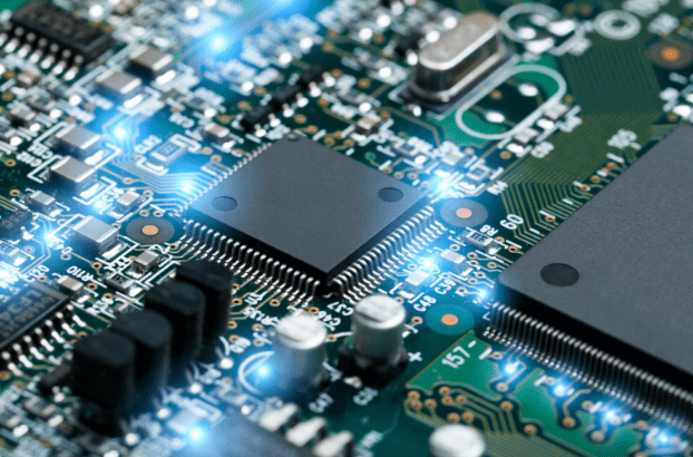
A printed circuit board turns separate parts into a stable system that powers up, talks to peripherals, and survives real world stress. The printed circuit board distributes power, guides signals with controlled impedance, anchors mechanical loads, and spreads heat so targets hold across life. I think that captures the role in one breath. And just like customer engagement platforms define how users stick with a product, the printed circuit board defines how every component sticks together to deliver that product reliably.
PCB at a glance
| Layer | Role | Typical materials | Design constraint | Validation focus |
| Top | Component breakout | Copper, FR4, solder mask | Escape density | AOI, X ray |
| Inner signal | High speed routes | Copper, prepreg | Impedance | TDR, eye scans |
| Ground plane | Return, shielding | Copper core | Continuity | EMI scans |
| Power plane | Rails, decoupling return | Copper core | IR drop | PDN sweeps |
| Thermal spreader | Heat flow | Copper, vias | Theta JA path | IR camera |
| Bottom | IO, test access | Copper, mask | Probe clearance | ICT |
How does a circuit board turn parts into a reliable system?
A circuit board achieves that with disciplined routing, solid reference planes, and a power network that stays quiet during transients. That mix protects timing, reduces noise, and stabilizes complex circuits inside an electronic device.
How do routing and stack up prove signal integrity at speed?
Routing and stack up prove signal integrity with controlled impedance copper traces, tight return paths, and clean via transitions that preserve eye height and width. Conclusive PCB design methods tighten skew and crosstalk limits through tuned pair lengths, reference continuity, and back drilled stubs. Differential pairs track together across copper layers and inner copper layers on multilayer pcbs. Modern printed circuit boards often add high density interconnect so integrated circuits and passive components fit without margin loss.
How does the power delivery network stay quiet during load steps?
The power delivery network stays quiet by meeting a target impedance across frequency and by placing bulk, mid, and high frequency capacitors near electronic components. Stitched planes and short current paths reduce droop during bursts. Developer guides that teach how to build web apps for device dashboards should note that high rate polling and OTA jobs raise transient demand, so PDN headroom matters when sensors and radios spike activity.
How does PCB design reduce emissions and heat in crowded enclosures?
PCB design reduces emissions and heat with continuous reference planes, minimal slots, purposeful stitching, and copper spreading tied into sinks through thermal vias. Notification spikes triggered through customer engagement platforms can cluster radio traffic, so keep return paths intact near radios and place decoupling at pins. Surface mount technology dominates component placement today, with through hole components used where mechanical strength or service matters.
What manufacturing, mechanics, and test work does the circuit board take on?
The printed wiring board supports manufacturability with clear rules for the manufacturing process such as adequate annular rings, clean solder mask dams, tuned paste apertures, accurate fiducials, and panelization that protects edges. The same printed circuit board PCB speeds test with accessible points, boundary scan hooks, bed of nails access, and power on sequences that isolate faults quickly. Mechanics count as well through connector retention, keep outs, strain relief, and stiffness that protect the mechanical structure during drop and vibration. Printed circuit board assembly choices span surface mount and mixed tech builds with hole components where needed. During printed circuit board manufacturing, material selection and copper thickness on a rigid substrate influence reliability and thermal expansion.
Which product level features does the printed circuit board enable?
A printed circuit board enables secure boot chains, clean sensor readouts next to switching power, RF coexistence across Wi Fi, LTE, and Bluetooth, and battery life that matches the model. That foundation also supports service access, firmware updates, and accessory connectors without tearing the unit apart. PCBs assign electrons reserved seats and a strict curfew.
Which functions does the circuit board centralize
- Power domains and local regulation across multiple layers
- Clock trees and resets guided by a robust PCB layout
- High speed IO lanes, connectors, and conductive pathways
- Isolation barriers, safety clearances, and non conductive substrate choices
- Thermal conduits to sinks or chassis with a sound construction method
- Test hooks, programming access, and bare board diagnostics
- HDI fan outs for dense surface mount parts and a surface mount device footprint
FAQs
What is the main function of a PCB?
A printed circuit board provides mechanical support and electrical interconnects, distributing power and routing signals so the product works reliably.
How does a PCB board work?
Copper traces and planes link components across laminated layers. Vias join layers, solder mask prevents bridges, and controlled geometry sets impedance and noise margins.
Why do you need a PCB?
You gain repeatable performance, compact assembly, and efficient manufacturing and test at scale.
Is PCB like a motherboard?
A motherboard is one specific printed circuit board for computers. Every motherboard is a PCB, not every PCB is a motherboard.